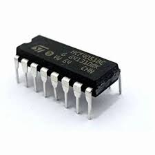
SD SMD HCF4051BE 8-channel Analog Multiplexer/Demultiplexer
The HCF 4051BE is a CMOS analog multiplexer/demultiplexer IC, part of the 4000 series. It features 8 channels, allowing it to switch one of eight inputs to a common output, or vice versa, controlled by a 3-bit binary address. It operates with a wide voltage range (3V to 20V) and is commonly used in signal routing, data acquisition, and analog signal processing.

The HCF 4051BE is a monolithic integrated circuit fabricated in MOS (Metal-Oxide-Semiconductor) technology. It is part of the 4000 series CMOS logic family, which is known for its low power consumption and wide operating voltage range. The HCF 4051BE is a single 8-channel analog multiplexer/demultiplexer, meaning it can route one of eight input signals to a common output or vice versa, depending on the configuration.
#Key Features:
1.8-Channel Analog Multiplexer/Demultiplexer: The IC can select one of eight analog or digital signals and route it to a single output, or it can take a single input and route it to one of eight outputs.
2.Low Power Consumption: As a CMOS device, it operates with very low power consumption, making it suitable for battery-powered applications.
3.Wide Operating Voltage Range: The HCF 4051BE can operate with a supply voltage ranging from 3V to 20V, providing flexibility in various electronic designs.
4.High Noise Immunity: CMOS technology provides high noise immunity, which is beneficial in environments with electrical noise.
5.Low ON Resistance: The IC has a relatively low ON resistance between the input and output, which minimizes signal attenuation.
6.Break-Before-Make Switching: This feature ensures that the current channel is disconnected before the new channel is connected, preventing any short-circuiting during switching.
7.Digital Control: The selection of the channel is controlled by three binary address inputs (A, B, and C), which can be driven by digital logic signals.
#Applications:
1.Analog Signal Routing: Used in audio and video signal routing, data acquisition systems, and communication systems.
2.Digital Signal Multiplexing: Can be used in digital systems to multiplex multiple digital signals onto a single line.
3.Sensor Arrays: Useful in applications where multiple sensors need to be read by a single analog-to-digital converter (ADC).
4.Test Equipment: Often used in test and measurement equipment to switch between different test points.
#Pin Configuration:
Pins 1, 2, 4, 5, 12, 13, 14, 15: Analog input/output channels (Y0-Y7).
Pin 3: Common output/input (Z).
Pins 9, 10, 11: Binary address inputs (A, B, C).
Pin 6: Inhibit input (INH), which when high, disables all channels.
Pin 7: VSS (Ground).
Pin 8: VEE (Negative supply voltage, typically ground in single-supply applications).
Pin 16: VDD (Positive supply voltage).
#Typical Use Case:
In a typical application, the HCF 4051BE might be used to multiplex several analog signals into a single analog-to-digital converter (ADC). The digital control pins (A, B, C) would be used to select which signal is currently being read by the ADC. This allows for efficient use of the ADC and reduces the number of components needed in the system.
#Summary:
The HCF 4051BE is a versatile and reliable IC for analog and digital signal multiplexing and demultiplexing. Its low power consumption, wide voltage range, and high noise immunity make it suitable for a wide range of applications in both consumer and industrial electronics.